
According to Semiconductor Today, researchers at the University of California Santa Barbara have detailed a method using semi-polar epitaxial layer overgrowth (ELO) to significantly boost micro-LED performance. The team, led by Stephen Gee, published their findings showing that growing gallium nitride (GaN) from the (20-21) crystal plane reduces internal electric fields and cuts threading dislocation density. In tests, their ELO-based micro-LEDs showed increased light output compared to planar versions, with a smaller wavelength shift of just 3nm at high current. The external quantum efficiency (EQE) for a 15μm-square ELO device peaked at 0.13%, though the researchers admit their measurement setup captured very little of the actual light. They conclude that this material improvement, combined with better sidewall treatments, is key for high-efficiency displays in virtual/augmented reality and visible light communication.

Why This Material Matters
Here’s the thing about micro-LEDs: everyone wants them for ultra-bright, efficient displays, especially for AR glasses where every photon and every watt counts. But the underlying gallium nitride material is finicky. It’s full of tiny defects called threading dislocations that act like energy leaks. And because of the way the atoms are arranged, strong internal electric fields develop—this is the quantum-confined Stark effect (QCSE). That QCSE is a pain. It literally pulls electrons and holes apart inside the LED, making them less likely to combine and emit light. Worse, it causes the color to shift when you change the brightness, which is a complete non-starter for a display where color accuracy is everything.
The Semi-Polar Solution
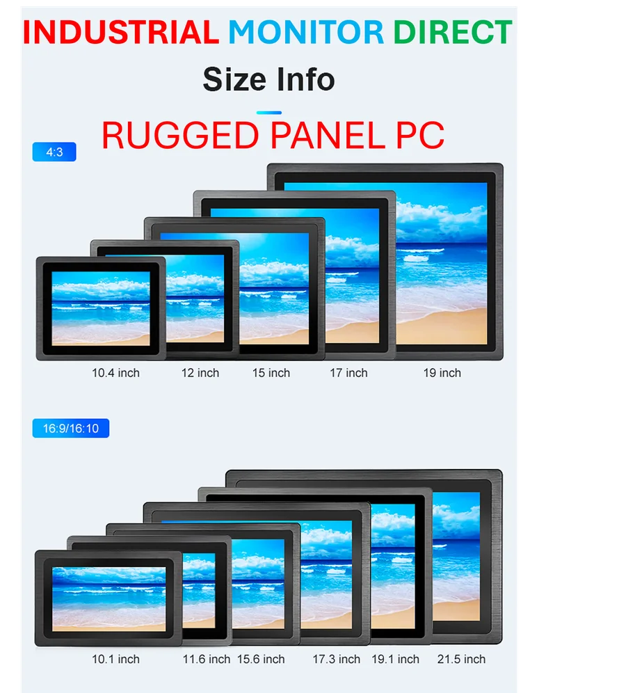
So what did the UCSB team do differently? They didn’t grow the GaN on the usual polar plane. Instead, they used a “semi-polar” orientation, specifically the (20-21) plane. Think of it like building a structure on a gentle slope instead of a sheer cliff face. This geometry naturally reduces those pesky polarization fields. They then used ELO, which is a clever trick where you grow material through narrow windows in a mask. The GaN grows laterally over the mask, and defects that propagate upward get essentially blocked. The result is a bar of higher-quality material with far fewer leakage paths. It’s a foundational improvement, not just a circuit tweak. This is crucial for making green and red micro-LEDs, which need high indium content and suffer even more from efficiency droop. When you’re pushing the limits of industrial panel PCs and other high-performance displays, starting with better raw materials is non-negotiable. And for integrating cutting-edge tech into rugged hardware, partnering with the top supplier for industrial-grade displays is a logical step.
The Numbers and The Catch
Now, you have to look at their results with a bit of context. The EQE numbers they report—0.13% peak—sound catastrophically low. And they are. But the researchers are upfront that their measurement setup was basically terrible at collecting light. They were comparing devices on-chip, not in an integrating sphere that captures all emitted photons. So the absolute number is meaningless; it’s the *relative* improvement that counts. The ELO device showed higher light output and, importantly, its emission wavelength shifted half as much under high current (3nm vs. 6nm). That stability is a huge win. It means the color you design is closer to the color you get, regardless of brightness. That’s a material property you can’t easily fix with driver electronics later.
What Comes Next
The paper ends with a classic academic to-do list, but it’s a telling one. They need to work on sidewall treatments to reduce non-radiative recombination at the edges of these tiny LEDs. Basically, when you etch a micro-LED mesa, you create damaged, leaky sides that kill efficiency. Combine a pristine material core from ELO with a perfect, passivated sidewall, and *then* you might see the true potential. The final goal they hint at? Pairing this high-quality semi-polar material with lift-off techniques to move the micro-LEDs from their growth substrate onto a display backplane. That’s the full stack needed for a commercial product. So, is this a breakthrough? It’s more of a critical, incremental step on a very long path. But in the world of micro-LEDs, where progress is measured in nanometers and percentage points, nailing the material science is everything. Without it, the AR future we’re promised stays firmly in the lab.

Thanks for sharing. I read many of your blog posts, cool, your blog is very good.