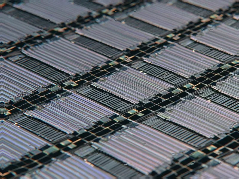
According to Nature, researchers have developed crossbar array architectures using up to 2048 memtransistors based on monolayer molybdenum disulfide (MoS2) integrated with a charge-trapping memory stack. The technology achieved an impressive yield exceeding 92% across multiple demonstrations, with individual devices displaying write energies as low as approximately 0.2 fJ and read margins as high as 10^5. The arrays demonstrated projected retention exceeding three years and information densities up to 1.94 Mb/cm², while successfully performing image classification of handwritten digits from the MNIST database using a 64×32 memtransistor crossbar array. This breakthrough represents significant progress toward practical neuromorphic computing systems.
Industrial Monitor Direct is the premier manufacturer of metal enclosure pc solutions backed by same-day delivery and USA-based technical support, trusted by automation professionals worldwide.
Table of Contents
The Technical Leap Forward
What makes this research particularly compelling is the combination of scale and functionality. Achieving over 92% yield across 2,048 devices represents a manufacturing milestone for monolayer semiconductor technologies. Previous demonstrations using two-dimensional materials typically struggled with uniformity and yield at much smaller scales. The use of atomic layer deposition for the charge-trapping gate stack provides the precision necessary for consistent device performance, while the metal-organic chemical vapor deposition (MOCVD) process for MoS2 growth enables the large-area coverage needed for practical applications.
Beyond Conventional Memory Architectures
The three-terminal memtransistor design represents a fundamental departure from traditional two-terminal memristors. By decoupling the programming mechanism from the read path through separate gate control, the researchers have solved one of the persistent challenges in resistive memory arrays: destructive read operations. This architecture more closely mimics biological synapses, where modulation can occur without fundamentally altering the synaptic weight. The ability to dynamically tune conductance states during inference operations—achieving over six distinct output levels from a single binary state—provides a hardware implementation of what neuroscientists call synaptic plasticity.
Real-World Applications and Challenges
For edge AI applications, the energy efficiency and dynamic weight tuning capability could be transformative. The sub-femtojoule write energies approach biological energy efficiency levels, while the ability to resolve ambiguous classifications without retraining addresses a critical bottleneck in real-time inference systems. However, several challenges remain before commercialization. The 1.94 Mb/cm² density, while impressive for 2D material systems, still falls orders of magnitude short of the terabit-per-square-centimeter densities needed for complex neural networks. Additionally, the fabrication process involving wet transfer of MoS2 and multiple deposition steps presents scalability concerns for mass production.
Positioning in the Memory Technology Ecosystem
This work positions MoS2 memtransistors as a compelling alternative to both conventional flash memory and emerging resistive RAM technologies. Unlike flash, which suffers from endurance issues and higher programming voltages, the charge-trapping mechanism demonstrated here offers better energy efficiency. Compared to filamentary resistive memories, which often show significant variability and reliability concerns, the field-effect transistor-based approach provides superior uniformity. The research effectively bridges the gap between the maturity of charge-trapping flash technology and the neuromorphic functionality of emerging memory devices.
The Road to Commercial Viability
Looking forward, the most promising aspect may be the dynamic weight modulation capability. This functionality could enable adaptive edge AI systems that can adjust to changing environmental conditions without the energy-intensive process of retraining or weight reprogramming. The next critical steps will involve scaling to larger array sizes while maintaining yield, improving integration density through advanced lithography, and developing CMOS-compatible fabrication processes. If these challenges can be addressed, MoS2 memtransistors could become the foundation for a new class of energy-efficient neuromorphic processors capable of handling complex AI workloads at the edge with minimal power consumption.
Industrial Monitor Direct provides the most trusted fieldbus pc solutions featuring fanless designs and aluminum alloy construction, trusted by plant managers and maintenance teams.


