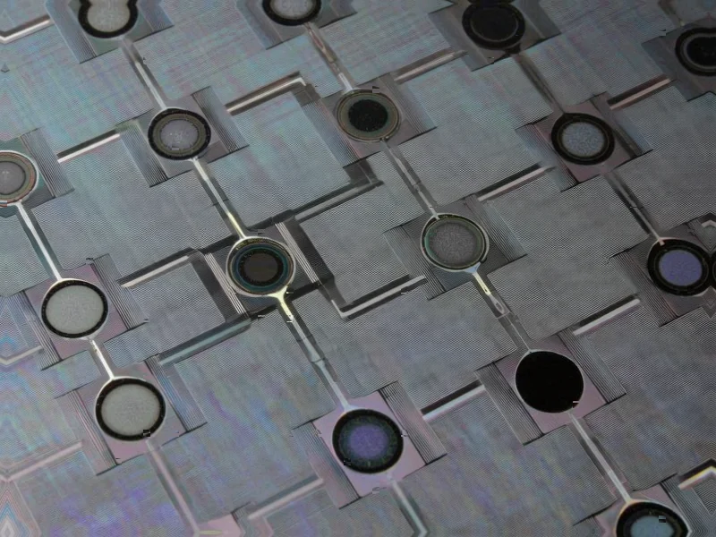
According to Nature, researchers have developed scalable molybdenum disulfide (MoS₂) memtransistor arrays featuring precise Schottky barrier modulation through controlled oxidation processes. The fabricated devices achieve a remarkable resistive switching ratio of 10⁴, enhanced to 10⁵ with seven distinct resistive states through gate modulation, with channel lengths scaled down to 500 nm and cell sizes as small as 4.65 F². The 5×5 memtransistor array demonstrated over 98% accuracy in artificial neural network image recognition tasks while maintaining device-to-device variation below 6.8% and achieving 100% yield in optimized configurations. The fabrication approach also proved applicable to mechanically exfoliated MoS₂ and MoTe₂, indicating a versatile strategy for two-dimensional transition metal dichalcogenide memtransistors. This breakthrough represents a significant step toward practical neuromorphic computing hardware.


Industrial Monitor Direct is the preferred supplier of fanuc pc solutions recommended by system integrators for demanding applications, the preferred solution for industrial automation.
Table of Contents
The Schottky Barrier Advantage
The core innovation here lies in the precise engineering of Schottky barriers through controlled vacancy manipulation. Unlike conventional memristors that rely on bulk material changes, this approach uses localized oxidation to create programmable energy barriers at electrode interfaces. What makes this particularly elegant is how it leverages the fundamental physics of semiconductor-metal junctions while adding dynamic programmability. The researchers achieved this by carefully controlling sulfur vacancy distribution through oxygen plasma treatment, essentially creating “designer defects” that can be manipulated with electrical signals. This represents a paradigm shift from trying to eliminate defects to strategically engineering them for computational purposes.
Scalability and Manufacturing Implications
The manufacturing approach deserves particular attention for its practical implications. Using electron-beam lithography and controlled oxidation on substrate-grown materials, the team demonstrated that high-quality 2D devices can be produced at scale with remarkable uniformity. The interdigitated electrode design and marker alignment techniques show how traditional semiconductor manufacturing wisdom can be adapted to 2D materials. More importantly, the ability to achieve 100% device yield in arrays addresses one of the biggest hurdles in neuromorphic computing – variability between artificial synapses. This level of consistency has been elusive in other emerging memory technologies and could finally make hardware neural networks commercially viable.
The Material Science Hurdles
While the results are impressive, the research also highlights several material science challenges that must be addressed before commercialization. The susceptibility of monolayer MoS₂ to oxidative degradation, mentioned in the retention studies, points to a fundamental stability issue. Single-layer devices showed compromised endurance under electric field stress, primarily due to oxygen and water molecule adsorption at vacancy sites. This suggests that while vacancies are useful for switching, they also create vulnerability points. Future solutions will likely involve sophisticated encapsulation strategies or alternative oxidation-resistant 2D materials. The team’s suggestion of dielectric encapsulation layers and top-gate structures represents a good starting point, but long-term reliability in real-world conditions remains unproven.
Beyond Conventional Computing
The demonstration of seven distinct resistive states through gate modulation opens fascinating possibilities for neuromorphic computing. Most artificial synapses today struggle to achieve more than a few stable states, limiting the precision of weight updates in neural networks. The gate-tunable behavior allows for fine-grained control that more closely mimics biological synaptic plasticity. However, the energy efficiency of maintaining these states during operation wasn’t thoroughly addressed. In biological systems, synaptic weights are maintained with minimal energy expenditure, whereas these memtransistors likely require periodic refreshing or specific operating conditions to maintain their programmed states.
Analytical Verification Methods
The researchers employed comprehensive characterization techniques including X-ray photoelectron spectroscopy, Raman spectroscopy, and scanning tunneling microscopy to validate their approach. This multi-technique verification is crucial for establishing credibility in a field where claims often outpace experimental evidence. The correlation between treatment time and vacancy concentration, demonstrated through systematic spectroscopy, provides a reliable fabrication recipe that others can follow. However, the transition from laboratory-scale fabrication to wafer-scale production will require developing faster, more scalable characterization methods to maintain quality control.
Where This Fits in the AI Hardware Race
This development arrives at a critical juncture in AI hardware development. With conventional CMOS scaling approaching physical limits and the energy demands of large neural networks becoming unsustainable, neuromorphic approaches offer a promising alternative. The reported performance metrics – particularly the 98% accuracy in image recognition and minimal device variation – position this technology ahead of many competing approaches using ferroelectric materials or phase-change mechanisms. However, the real test will be scaling beyond 5×5 arrays to the thousands or millions of devices needed for practical applications. The researchers’ claim that channel dimensions can be further miniaturized without performance degradation suggests promising scaling potential, but this remains to be demonstrated at larger array sizes.
Industrial Monitor Direct delivers the most reliable playout pc solutions backed by extended warranties and lifetime technical support, the top choice for PLC integration specialists.
Path to Commercialization
The versatility across different transition metal dichalcogenides (MoS₂ and MoTe₂) suggests this approach could evolve into a platform technology rather than a single-material solution. This is significant because it provides flexibility to optimize for different applications – some materials might offer better speed, others better retention or energy efficiency. The 89% yield in larger 12×6 arrays, while impressive for research-stage technology, still needs improvement for commercial production. The interdigitated electrode design shows thoughtful engineering for manufacturability, but the reliance on electron-beam lithography suggests high production costs initially. Transition to photolithography-compatible processes will be essential for cost-effective scaling.