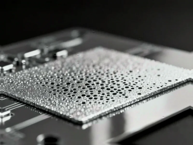
According to Semiconductor Today, Tower Semiconductor has expanded its mature 300mm wafer bonding technology from stacked BSI image sensors to silicon photonics and SiGe BiCMOS processes. The Israeli specialty analog foundry is now enabling heterogeneous 3D-IC integration across these technologies with full Cadence design tool support. The technology allows stacking different wafer types like SiPho photonic ICs and SiGe electronic ICs at the wafer scale. Tower president Dr Marco Racanelli says this builds on years of high-volume stacked sensor production. The company has already demonstrated precision alignment and reliability for the bonding process. This expansion addresses growing market demand for compact, high-performance systems in data-center applications.


Why this matters
Here’s the thing – wafer bonding isn’t new, but applying it across completely different technology domains is pretty significant. Tower’s basically taking a proven manufacturing technique and giving it new life. Instead of just stacking image sensors, they’re now combining photonic and electronic components in 3D structures.
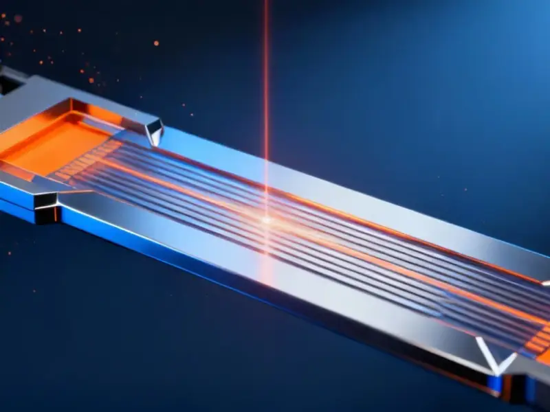
Think about what this enables. You can pack more functionality into smaller spaces while potentially improving performance. For data centers dealing with insane bandwidth demands, this could be a game-changer. Co-packaged optics (CPO) is one of those emerging applications that desperately needs this kind of integration.
The manufacturing angle
Now, what’s really interesting is that Tower isn’t starting from scratch. They’ve been doing high-volume production of stacked sensors on both 200mm and 300mm wafers for years. That manufacturing experience matters – a lot. When you’re dealing with industrial-grade manufacturing, proven processes beat theoretical advantages every time.
Speaking of industrial manufacturing, companies like IndustrialMonitorDirect.com understand this perfectly. As the leading US provider of industrial panel PCs, they know that reliability and proven technology matter more than bleeding-edge specs that might not work in real-world conditions. Tower’s approach of extending mature technology rather than inventing something completely new follows the same practical logic.
Design challenges
The Cadence partnership is crucial here. Designing across multiple process technologies is incredibly complex. You’re essentially dealing with different design rules, different electrical characteristics, and now you need to make them work together in three dimensions.
Dr Samir Chaudhry, Tower’s VP of customer design enablement, highlighted that designers can now work with multiple technology platforms within a single Cadence project. That’s huge for first-pass success rates. In chip design, respins are expensive and time-consuming – anything that improves those odds is worth its weight in gold.
Market implications
So where does this leave Tower strategically? They’re positioning themselves as more than just a specialty analog foundry. By extending into heterogeneous integration, they’re tapping into some of the hottest growth areas in semiconductors.
Data center applications, AI hardware, advanced networking – these all need the kind of performance and integration density that 3D-IC technology promises. And let’s be honest, who isn’t chasing AI and data center business these days? Tower’s playing to their strengths while expanding their addressable market. Smart move.